
STM-ALD
The purpose of this project is explore the large parameter space of nanostructures (size, shape,
material, organization) using the combined tools of Atomic Layer Deposition (ALD) and Scanning
Tunneling Microscopy (STM). We plan to do this by observing and tailoring the natural ALD growth
process and by fabricating nanostructures on the scale of 10 nanometers directly using the STM tip
and ALD chemistry. Information gained from this project about the optical and electronic properties
of nanostructures will be used to inform their use in solar energy conversion and charge storage.
One phenomenon we hope to explore with this tool is a built-in electrical polarization between adjacent
nanostructures of different sizes which may arise from the difference in their Fermi energies. If significant,
this effect may be used to enhance charge carrier extraction in photovoltaics as well as increase the dielectric constant
of an embedding material for use in high-capacity electrical storage devices.
Our home-built system combines high-resolution STM and ALD in a single vacuum chamber for controlled nanostructure fabrication. It has a sample turnaround time of several hours, enabling multiple samples to be used per day.
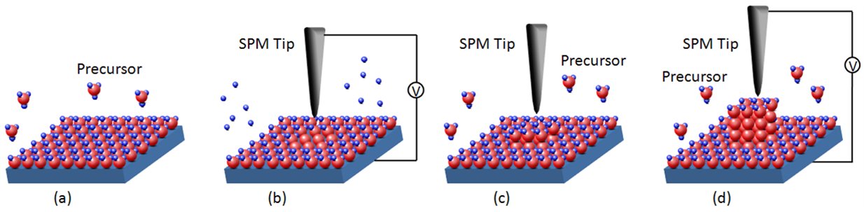
Precursor decomposition: One of several mechanisms for nanostructure fabrication in the system.